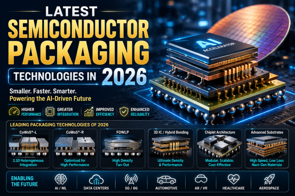
Latest-semiconductor-packaging-technologies-2026
Discover the latest semiconductor packaging technologies shaping AI in 2026, including HBM, chiplets, co-packaged optics, hybrid bonding, and advanced substrates.
Advanced packaging is rapidly becoming one of the most important growth engines in the semiconductor industry. This week’s developments show why packaging, integration, and system architecture now matter more than ever for AI and high-performance computing.
# Latest Semiconductor Packaging Technologies in 2026: Why Advanced Packaging Is Driving AI Growth
The semiconductor industry is entering a new phase where advanced packaging is no longer just a back-end manufacturing step. It is now becoming one of the key drivers of innovation in artificial intelligence, high-performance computing, and next-generation processors.
Recent developments reported over the last few days by reliable industry sources such as Semiconductor Engineering, SEMI, DIGITIMES, and Advanced Packaging News all point to the same conclusion: the future of semiconductor performance will depend not only on transistor scaling, but also on packaging technology, heterogeneous integration, and system-level design.
This is a major shift, and it matters greatly for engineers, semiconductor professionals, and technology leaders.
## Why Advanced Packaging Matters More Than Ever
For many years, semiconductor progress was mainly associated with shrinking transistor sizes. That model is still important, but it is no longer enough on its own. Today’s AI systems demand more bandwidth, more memory, better thermal performance, lower power consumption, and higher integration density.
That is exactly where advanced packaging comes in.
Technologies such as 2.5D integration, 3D stacking, chiplets, high-bandwidth memory (HBM), co-packaged optics, hybrid bonding, and advanced substrates are allowing the industry to create powerful systems that go beyond the limits of traditional single-die design.
In simple terms, packaging is becoming a core part of system architecture.
## ECTC 2026 Shows the Direction of Travel
One of the clearest signals came from coverage of ECTC 2026. According to Semiconductor Engineering, this year’s conference highlighted how packaging technologies are redefining the scalability limits of AI and HPC.
Among the major themes were:
– EMIB-T for large multi-die systems
– Co-packaged optics for higher bandwidth and lower power
– Glass substrates for larger form factors and improved stability
– Advanced HBM interconnect performance
This matters because AI accelerators and HPC systems increasingly require multiple dies, massive memory bandwidth, and strong signal integrity. Advanced packaging is what makes that possible.
## HBM Growth Is Also a Packaging Story
Another strong industry signal came from SEMI, which reported on June 30 that global 300mm memory equipment investment is expected to exceed US$50 billion in 2026, supported by demand for DRAM, HBM, and DDR5.
I can still recall the early days of DRAM when I was doing DRAM assembly and test in Siemens Melaka, Malaysia. Industry was transitioning from 4Mbit to 16 Mbit, and from alloy42 to copper leadframes. Package then was SOJ.
Now Memory has grown into a huge beast called HBM. HBM is not just a memory technology trend. It is also a packaging challenge and opportunity.
HBM performance depends heavily on:
– High-density interconnects
– Advanced thermal management
– Package-level signal integrity
– Reliable integration
– DIGITIMES:
https://www.digitimes.com/tag/tsmc/001264.html
https://www.digitimes.com/tag/sk_hynix/0017883.html
– Advanced Packaging News:
https://advancedpackaging.news/article/124287/ECTC_2026_spotlights_advanced_packaging
Cheerio. See you in my next blog – Harry Kam